


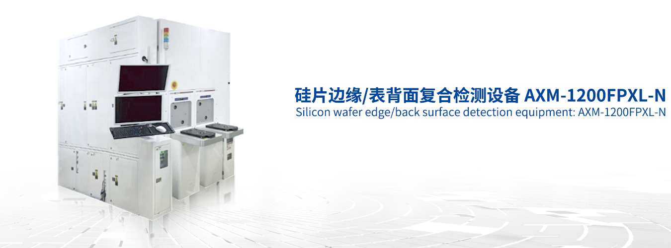
硅片边缘/表背面复合检测设备 AXM-1200FPXL-N
优点介绍
得到国际&国内客户端认可的量产型缺陷检测设备
晶圆片边缘&正背面全方位检测,最小检测缺陷0.2um
特有的Notch检测模块,做到Notch全域检测
自研缺陷检测算法,自动缺陷检测(AOI)和自动缺陷分类(ADC)
标准化检测单元,多模块组合,支持定制化结合
自研晶圆边缘夹持定位检测,减少对晶圆片二次污染和损伤
Mass production defect detection equipment recognized by international and domestic clients
Full directional inspection of the edge and front and back of the wafer, with a minimum detection defect of 0.2um
Unique Notch detection module, achieving Notch global detection
Self developed defect detection algorithm, automatic defect detection (AOI) and automatic defect classification (ADC)
Standardized detection unit, multi module combination, supporting customized combination
Self developed wafer edge clamping and positioning detection to reduce secondary pollution and damage to the wafer
参数配置
搭载自有专利的激光检测器+5台高速线性相机实现晶圆的边缘检测搭载自研光学架构和光学系统实现正背面缺陷检测
搭载4台高性能相机对Notch部全域监控
新功能(Auto.2D review)可以作为选配
搭配双port或多port EFEM单元对接OHT&AMR
Equipped with a patented laser detector and 5 high-speed linear cameras to achieve edge detection of wafers
Equipped with self-developed optical architecture and optical system to achieve front and back defect detection
Equipped with 4 high-performance cameras for full area monitoring of Notch department
The new feature (Auto.2D review) can be optional
Paired with dual or multi port EFEM units for OHT&AMR docking
功能描述
适用产品:半导体用12寸晶圆
适用工艺段:倒角 / 表面研磨 / 表面抛光 / 清洗 / 干燥 / PW终检 / Epi 、SOI等
功能说明:1.EFEM单元支持FOSB/FOUP/OC等人工或OHT上料
2.晶圆的边缘+正背面+Notch部全方位缺陷检测
3.缺陷类型包括: Scratch、Particle、Cloud、Grind Mark(SG)、Dirty 、Haze、Pin mark、Halo、 Crack、Chip等
Applicable products: 12 inch wafers for semiconductors
Applicable process segments: chamfering/surface grinding/surface polishing/cleaning/drying/PW final inspection/Epi, SOI, etc
Function Description:
1. The EFEM unit supports manual or OHT loading such as FOSB/FOUP/OC
2. Comprehensive defect detection of the edge, front andback, and Notch parts of the wafer
3. Defect types include: Scratch, Particle, Cloud, Grind Mark (SG), Dirty, Haze, Pin mark, Halo, Crack, Chip, etc

