


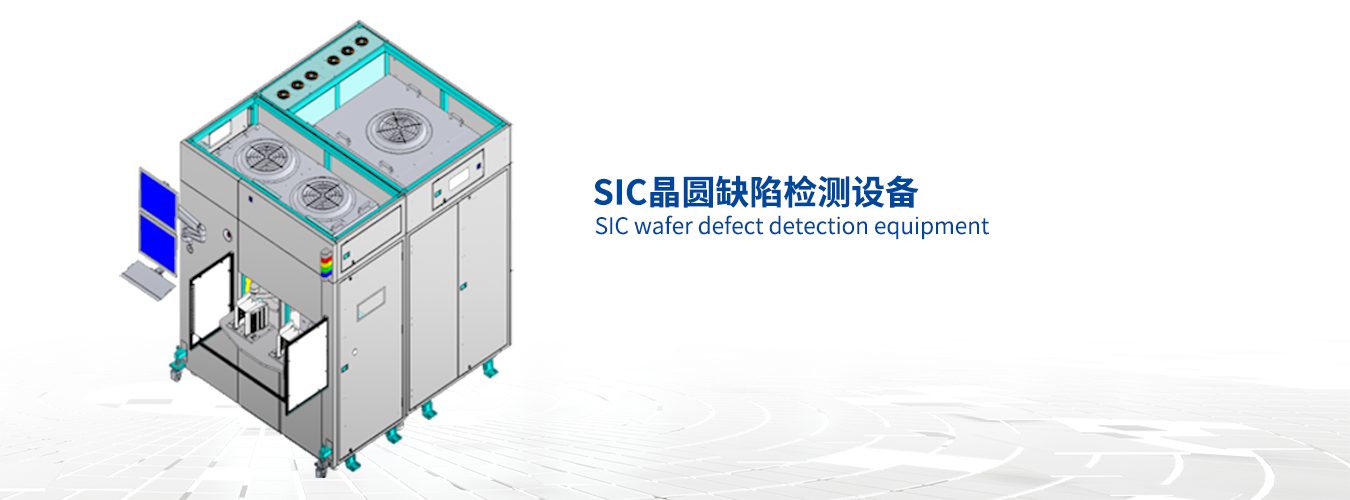
SIC晶圆缺陷检测设备
优点介绍
SIC缺陷检测设备测试验证数据已得到国内外客户认可
采用高速高性能线性相机,支持多种倍率切换
采用明场、暗场、PL、DIC视觉技术,检测多种缺陷
检测精度10um
The testing and verification data of SIC defect detection equipment has been recognized by domestic and foreign customers
Adopting high-speed and high-performance linear cameras, supporting multiple magnification switching
Using bright field, dark field, PL, and DIC visual technology to detect various defects
Detection accuracy of 10um
参数配置
搭载高清相机实现对晶圆位置自动引导定位采用高精度激光显微镜利用20X/50X物镜对倒角粗糙度自动扫描测量
搭配双port或多port EFEM单元对接OHT&AMR实现全自动上下料
Equipped with high-definition camera to achieve automatic guidance and positioning of wafer position
Automatic scanning measurement of chamfer roughness using a high-precision laser microscope and 20X/50X objective lens
Paired with dual or multiple port EFEM units to dock with OHT&AMR for fully automatic loading and unloading
功能描述
适用产品:半导体6/8寸SIC晶圆适用工艺段:倒角 / 表面研磨 / 表面抛光 / 清洗 / 终检等
功能说明:
1.EFEM单元支持FOSB/FOUP/OC等人工或OHT上料
2.晶圆的边缘+正背面
3.自主研发的缺陷检测算法,对缺陷自动检测,分析,并进行缺陷分类
4.缺陷类型包括:Downfall、Triangle、Carrot、Micropipe、IGSF、Bar SF、SF、BPD、Particle、Pit、Scratch等
Applicable products: Semiconductor 6/8-inch SIC wafers
Applicable process segments: chamfering/surface grinding/surface polishing/cleaning/final inspection, etc
Function Description:
1. The EFEM unit supports manual or OHT feeding of FOSB/FOUP/OC and other materials
2. Edge of wafer+front and back sides
3. Independently developed defect detection algorithm that automatically detects, analyzes, and classifies defects
4. Defect types include Downfall, Triangle, Carrot, Micropipe, IGSF, Bar SF, SF, BPD, Particle, Pit, Scratch, etc

