股票简称:赛腾股份
股票代码:603283
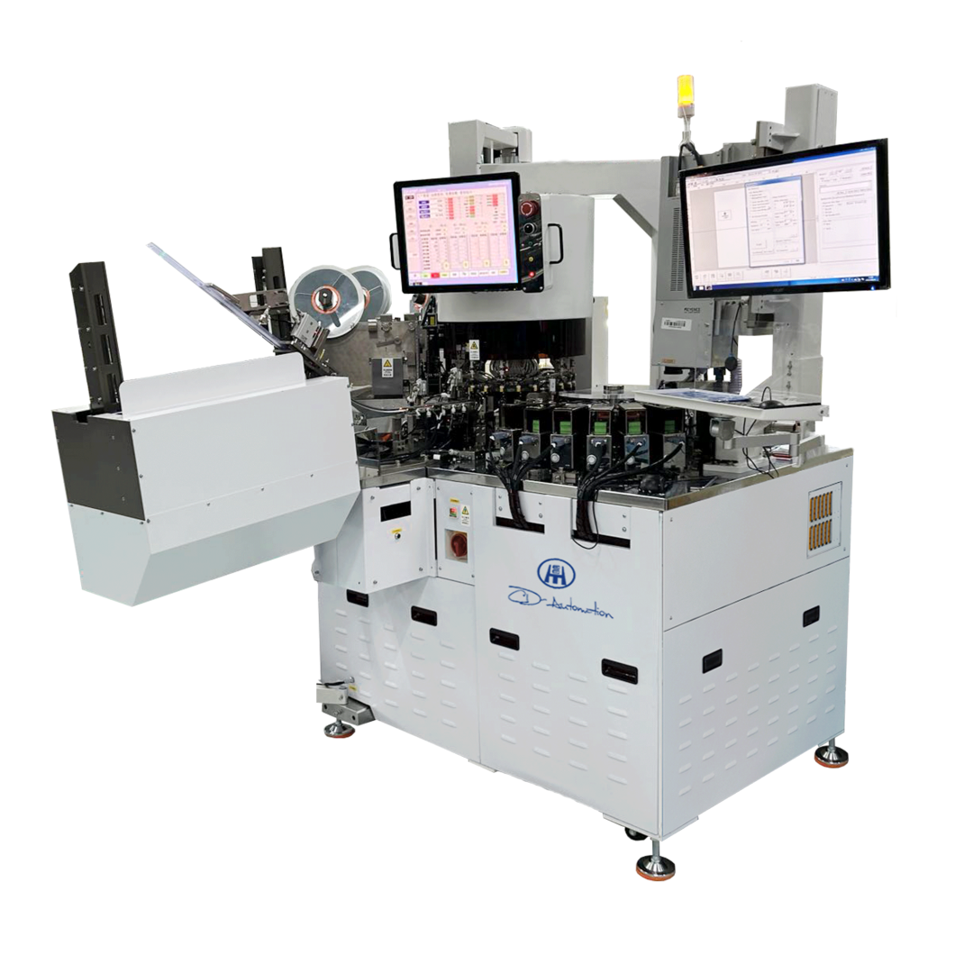
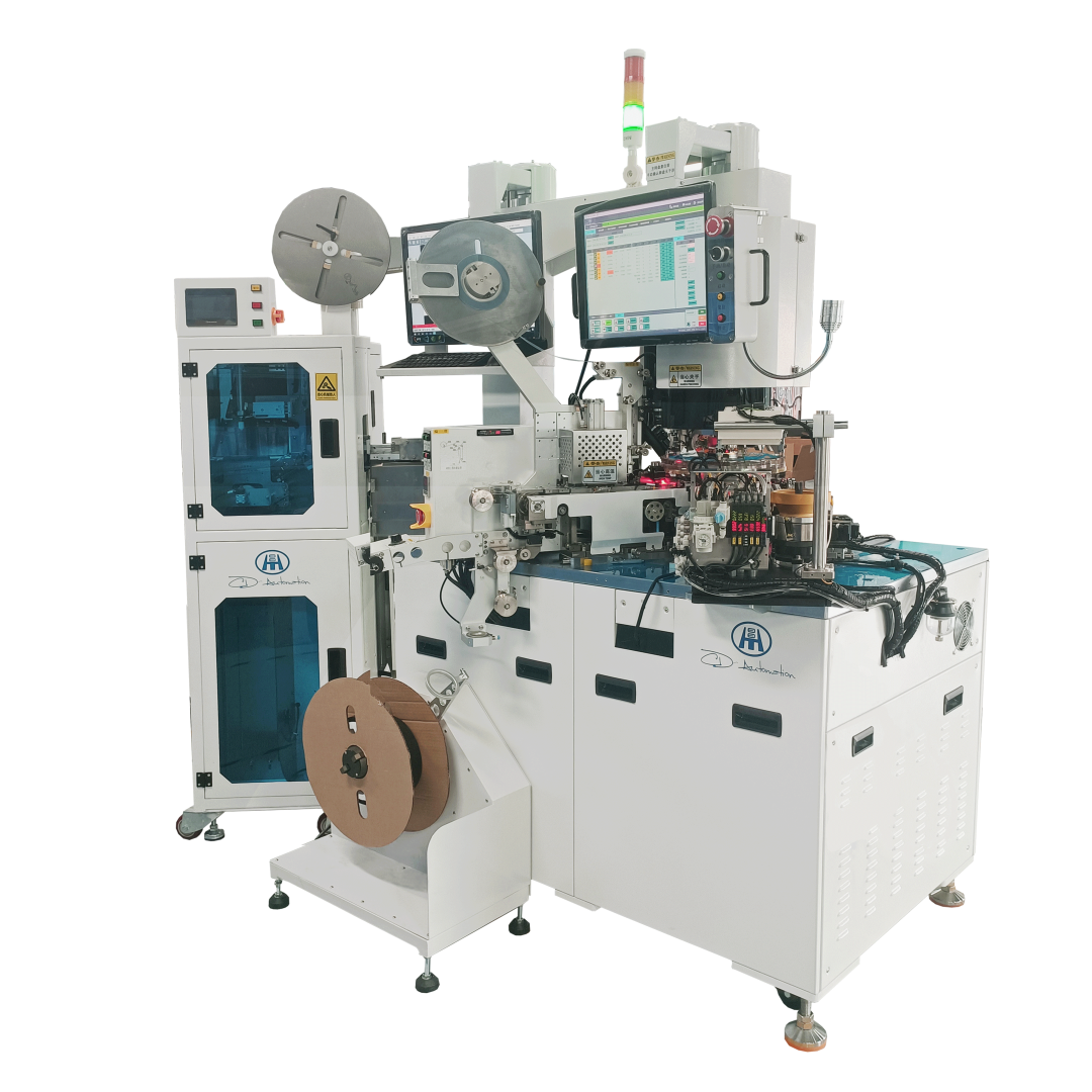
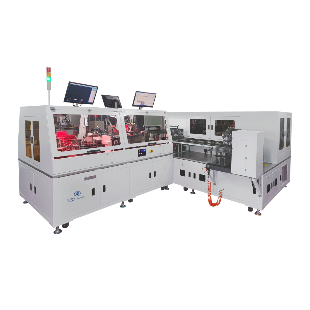
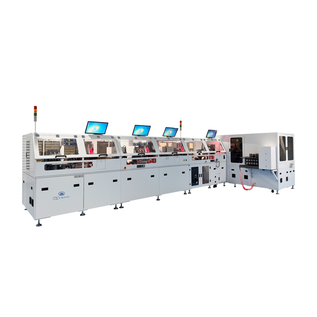
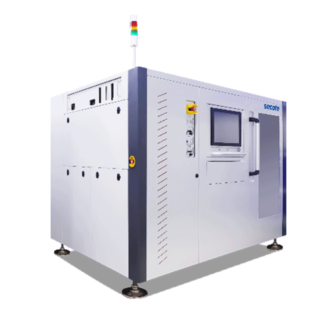
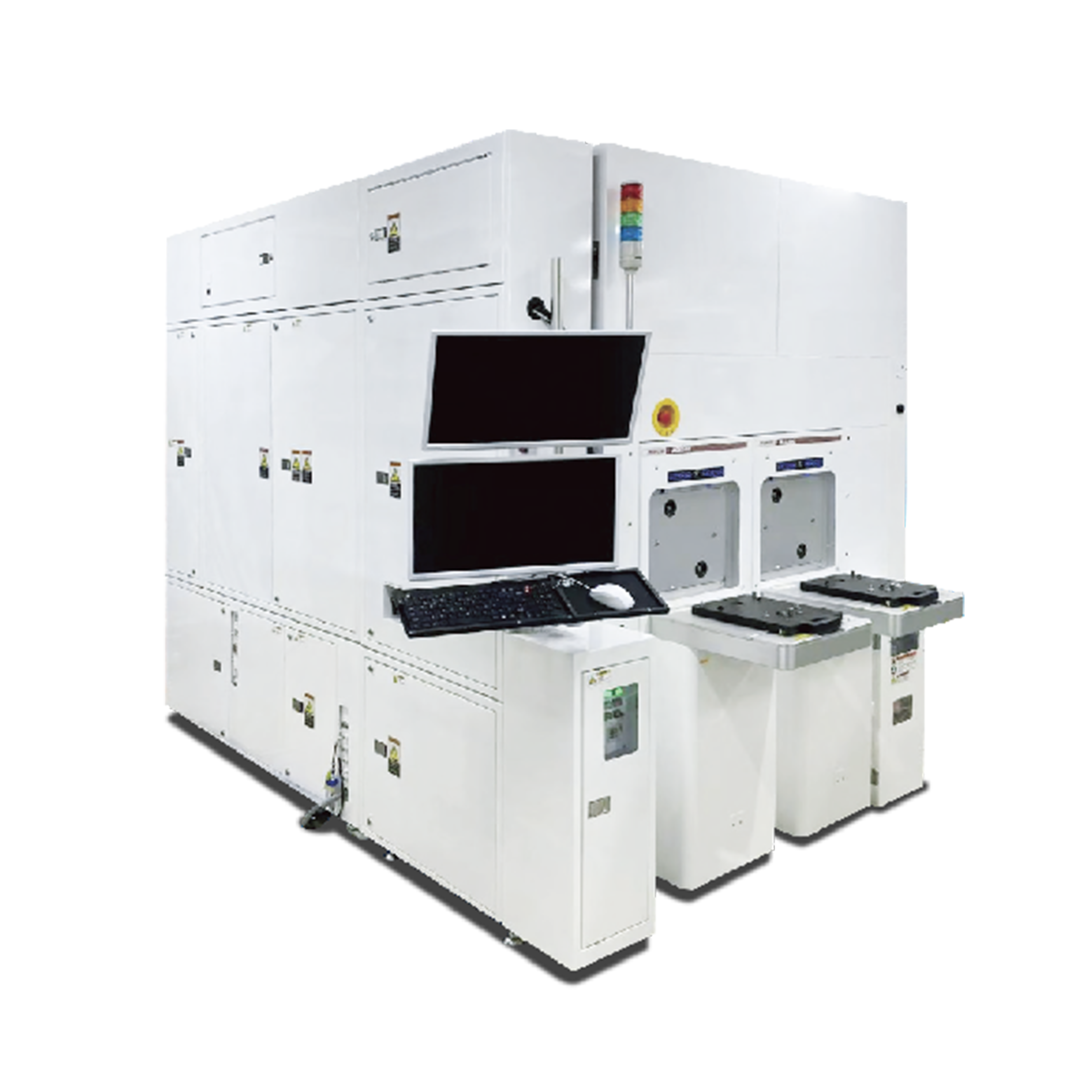
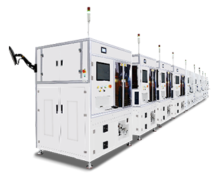
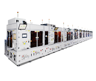
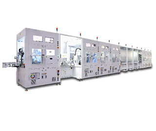
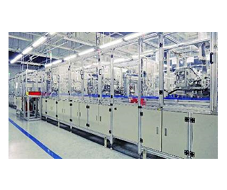
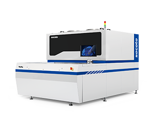
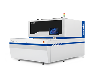
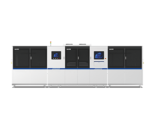
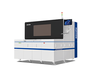
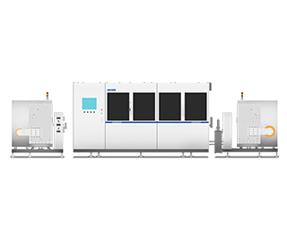
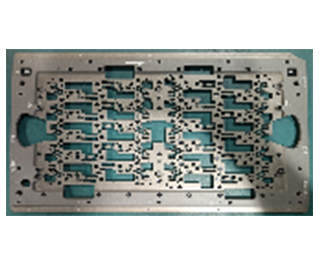
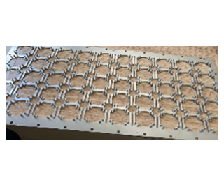
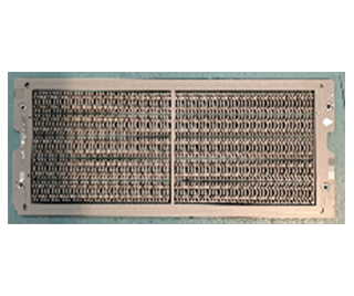
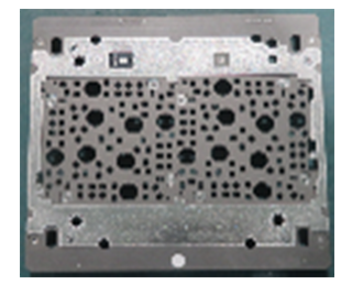
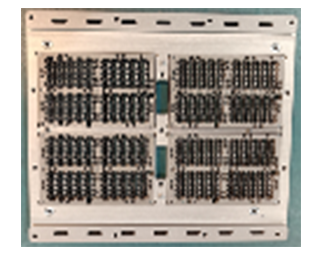
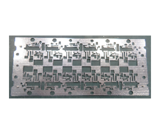
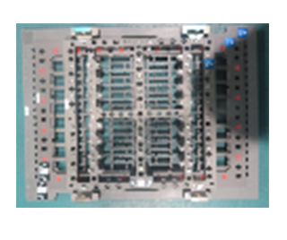
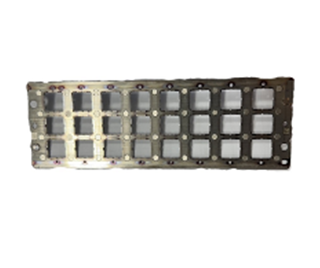
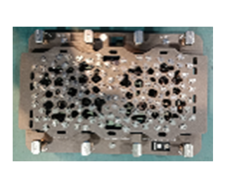
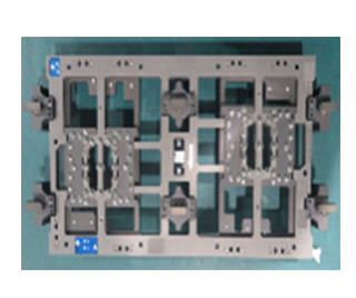
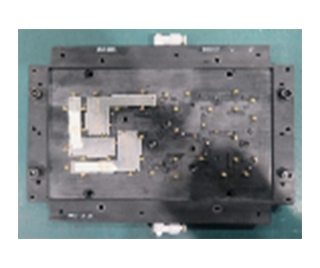
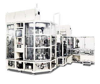
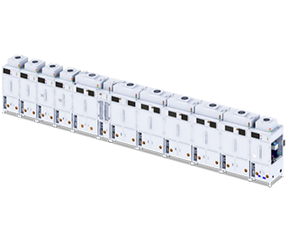
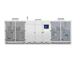
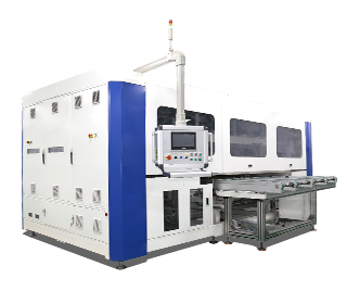
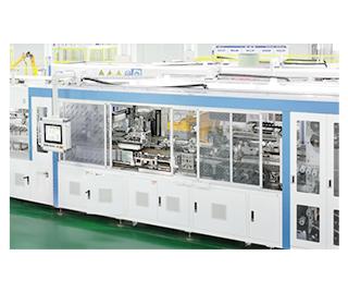
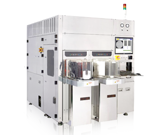
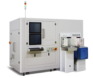
公司提供自动化解决方案,集非标自动化领域研发方案设计、精密加工、组装调试...
真诚合作,彼此互信!
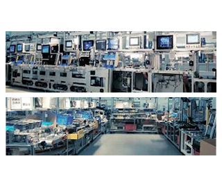
公司拥有T3级别机房,建立了以SAP系统为核心的信息化体系...
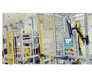
公司高度重视产品质量的检测与控制, 运用国际质量管理工具对产品进行质量管控...
24小时在线服务,第一时间为客户排忧解难..
强大的营销和售后网络遍布全球,为您保驾...
公司倡导环保理念,为客户设计节能环保产品,为履行环境责任和社会可持续发...
赛腾积极为员工提供岗位培训和职业发展机会,并为员工及其家属提供全方位的关爱计划...
公司倡导环保理念,为客户设计节能环保产品,为履行环境责任和社会可持...
欢迎每一位有梦想的人加入赛腾...