


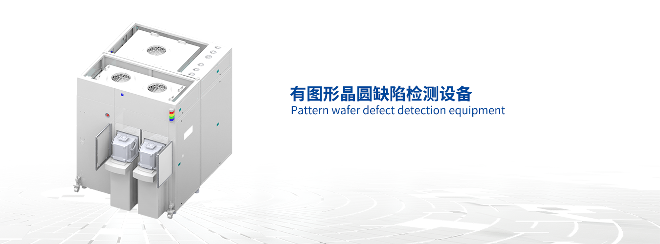
有图形晶圆缺陷检测设备
优点介绍
2x/5x/10x/20x/50x多倍率物镜自动切换
黑白/彩色双光路设计
明场/暗场检测模式
高精度自动对焦,兼容不同高度差异
检测精度0.1um
2x/5x/10x/20x/50x multi magnification objective lens automatic switching
Black and white/color dual light path design
Bright/dark field detection mode
High precision autofocus, compatible with different height differences
Detection accuracy 0.1um
参数配置
搭载黑白/彩色2种高清相机采用高速飞拍技术、高精度移动平台实现缺陷快速检测
自动复检(ADR)+ 自动缺陷分类(ADC)
搭配双port或多port EFEM单元对接OHT&AMR实现全自动上下料
Equipped with two high-definition cameras, black and white/color
Using high-speed aerial photography technology and high-precision mobile platform to achieve rapid defect detection
Automatic Re inspection (ADR)+Automatic Defect Classification (ADC)
Paired with dual or multiple port EFEM units to dock with OHT&AMR for fully automatic loading and unloading
功能描述
适用产品:半导体8/12寸有图形晶圆适用工艺段:薄膜沉积、光刻胶、激光开槽、划片切割等
功能说明:
1.EFEM单元支持FOSB/FOUP/OC等人工或OHT上料
2.黑白相机高速飞拍
3.彩色相机自动复检,缺陷自动分类
4.缺陷类型:Scratch、Crack、Particle、色差、划偏、金属残留、金属缺失、脏污、Die丢失、脱落等
Applicable products: Semiconductor 8/12 inch patterned wafer
Applicable process segments: Thin film deposition, photoresist, laser slotting, wafer cutting, etc
Function Description:
1. The EFEM unit supports manual or OHT automatic feeding such as FOSB/FOUP/OC
2. High speed aerial photography with black and white camera
3. Automatic re inspection of color cameras and automatic classification of defects4. Defect types: Scratch, Crack, Particle, color difference, scratch deviation, metal residue, metal missing, dirt, Die loss , detachment, etc

