


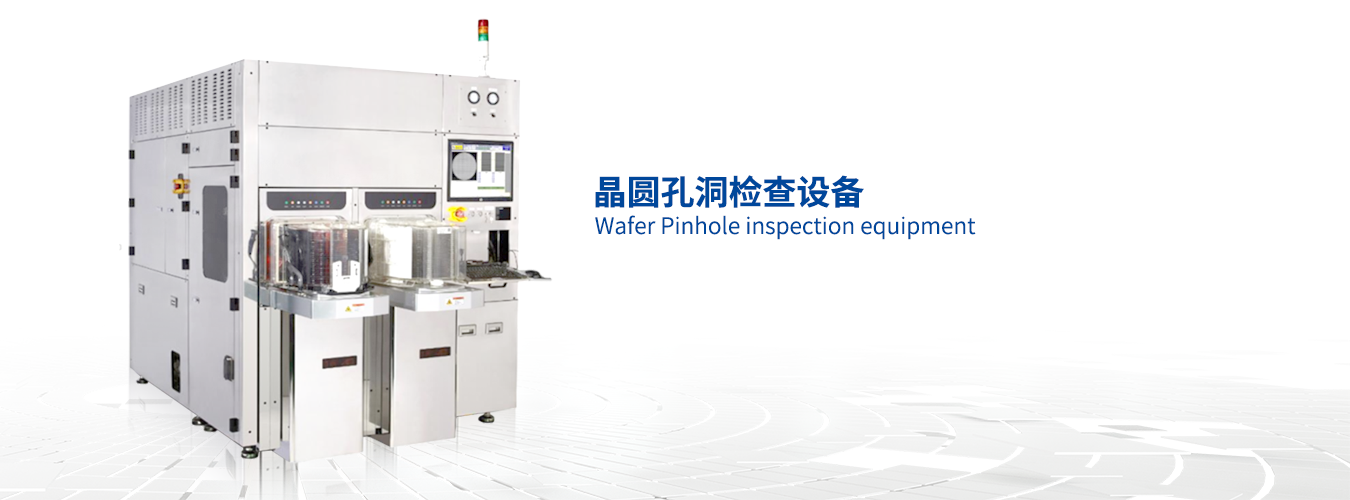
晶圆孔洞检查设备
优点介绍
得到国际&国内客户端认可的量产型缺陷检测设备
Throughput达到144WPH自动缺陷Review(ADR)和自动缺陷分类(ADC)
自研缺陷检测算法+深度学习结合,自动缺陷检测(AOI)和自动缺陷分类(ADC)
内部 + 表面晶圆缺陷检测可同时检测
Mass production defect detection equipment recognized by international and domestic clients
Throughput reaches 144WPH
Automatic Defect Review (ADR) and Automatic Defect Classification (ADC)
Self developed defect detection algorithm combined with deep learning, automatic defect detection (AOI) and automatic defect classification (ADC)
Internal and surface wafer defect detection can be performed simultaneously
参数配置
采用红外相机扫描穿透系统自主设计特殊的红外光源和红外摄像头提高了晶圆内部缺陷的捕获率
搭载高清复检相机对缺陷精确判定
搭配双port或多port EFEM单元对接OHT&AMR实现全自动上下料
Adopting an infrared camera scanning penetration system
Independently designed special infrared light source and infrared camera improve the capture rate of internal defects in wafers
Equipped with high-definition re inspection camera for precise defect detection
Paired with dual or multiple port EFEM units to dock with OHT&AMR for fully automatic loading and unloading
功能描述
适用产品:半导体12寸晶圆适用工艺段:倒角 / 表面研磨 / 表面抛光 / 清洗 / 干燥 / PW终检 / Epi 、SOI等
功能说明:
1.EFEM单元支持FOSB/FOUP/OC等人工或OHT上料
2.晶圆内部+表面的孔洞缺陷检测
3.自主研发的缺陷检测算法,对缺陷自动检测,分析,并进行缺陷分类
4.缺陷类型包括: Crack、Pit、PinHole等
Applicable products: 12 inch semiconductor wafers
Applicable process segments: chamfering/surface grinding/surface polishing/cleaning/drying/PW final inspection/Epi, SOI, etc
Function Description:
1. The EFEM unit supports manual or OHT feeding of FOSB/FOUP/OC and other materials
2. Defect detection of pores inside and on the surface of crystal grains
3. Independently developed defect detection algorithm that automatically detects, analyzes, and classifies defects
4. Defect types include: Crack, Pit, PinHole, etc

