


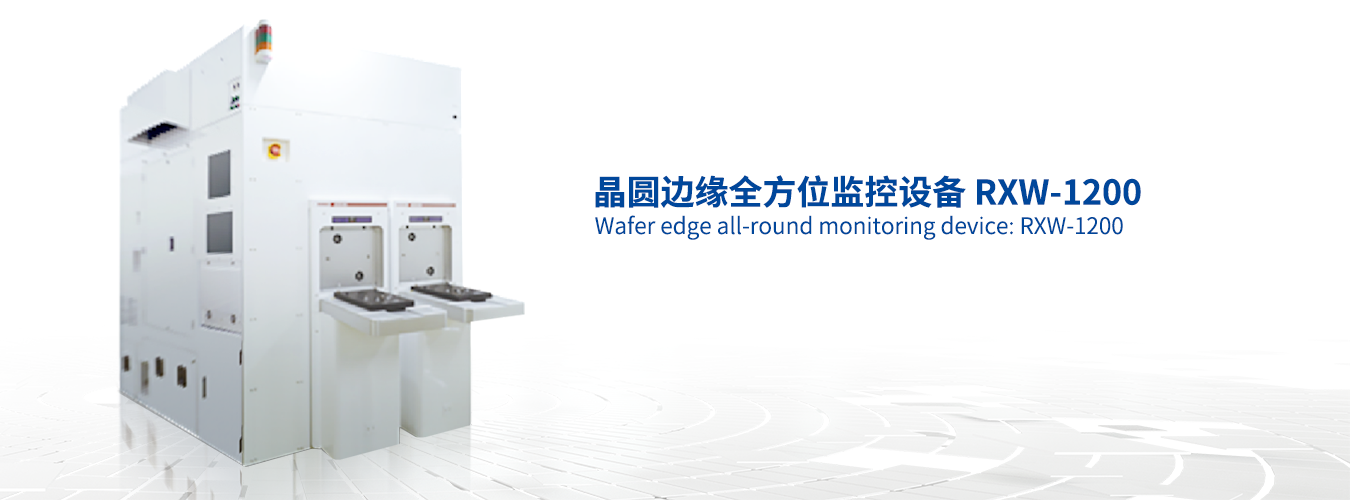
晶圆边缘全方位监控设备 RXW-1200
优点介绍
得到国际&国内客户端认可的全方位边缘监控设备
自研缺陷检测算法+深度学习结合,自动缺陷Review(ADR)和自动缺陷分类(ADC)
在线220度Review Inspection ,输出彩色图像
晶圆片边缘全方位检测,最小检测缺陷0.2um
同时实现边缘缺陷检测,厚度量测,边缘尺寸量测
A comprehensive edge monitoring device recognized by international and domestic clients
Combining self-developed defect detection algorithm with deep learning, automatic defect review (ADR) and automatic defect classification (ADC)
Online 220 degree Review Inspection, outputting color images
Omni directional detection of wafer edges, with a minimum detection defect of 0.2um
Simultaneously achieving edge defect detection, thickness measurement, and edge size measurement
参数配置
搭载自有专利的激光检测器+5台高速线性相机实现晶圆的边缘检测搭载自研光学架构和光学系统实现尺寸量测
准直投影成像技术对Edge Profile进行测量分析
集成式EFEM, 设备尺寸更小
设备已通过SEMI认证
Equipped with a patented laser detector and 5 high-speed linear cameras to achieve edge detection of wafers
Equipped with self-developed optical architecture and optical system for size measurement
Measurement and analysis of Edge Profile using collimated projection imaging technology
Integrated EFEM with smaller device size
The device has passed SEMI certification
功能描述
适用产品:半导体用12寸晶圆, W2W bonding晶圆适用工艺段: CIS工艺 / TSV工艺 / HBM工艺
功能说明:
1.EFEM单元支持FOSB/FOUP/OC等人工或OHT自动上料
2.晶圆的边缘缺陷检测和尺寸量测全方位监控
3.缺陷类型包括:Scratch、Crack、Chip、Dirty 、Bubble 、chipping 、Gathering of small dot 、Pit 、Flake 、Polymer Residue 、Peel等
4.量测包括:晶圆厚度、 Bonding后的边缘轮廓、切断高度、宽度的测量、Wafer是否对齐、 Notch是否对准等
Applicable products: 12 inch wafers for semiconductors, W2W bonding wafer
Applicable process segments: CIS process/TSV process/HBM process
Function Description:
1. The EFEM unit supports manual or OHT automatic feeding such as FOSB/FOUP/OC
2. Comprehensive monitoring of edge defect detection and size measurement of wafers
3. Defect types include: Scratch Crack, Chip, Dirty, Bubble, Chipping, Gathering of small dots, Pit, Flake, Polymer Reside, Peel, etc
4. Measurement includes: wafer thickness Measurement of edge contour, cutting height, and width after bonding Is the Wafer aligned Notch alignment, etc

