


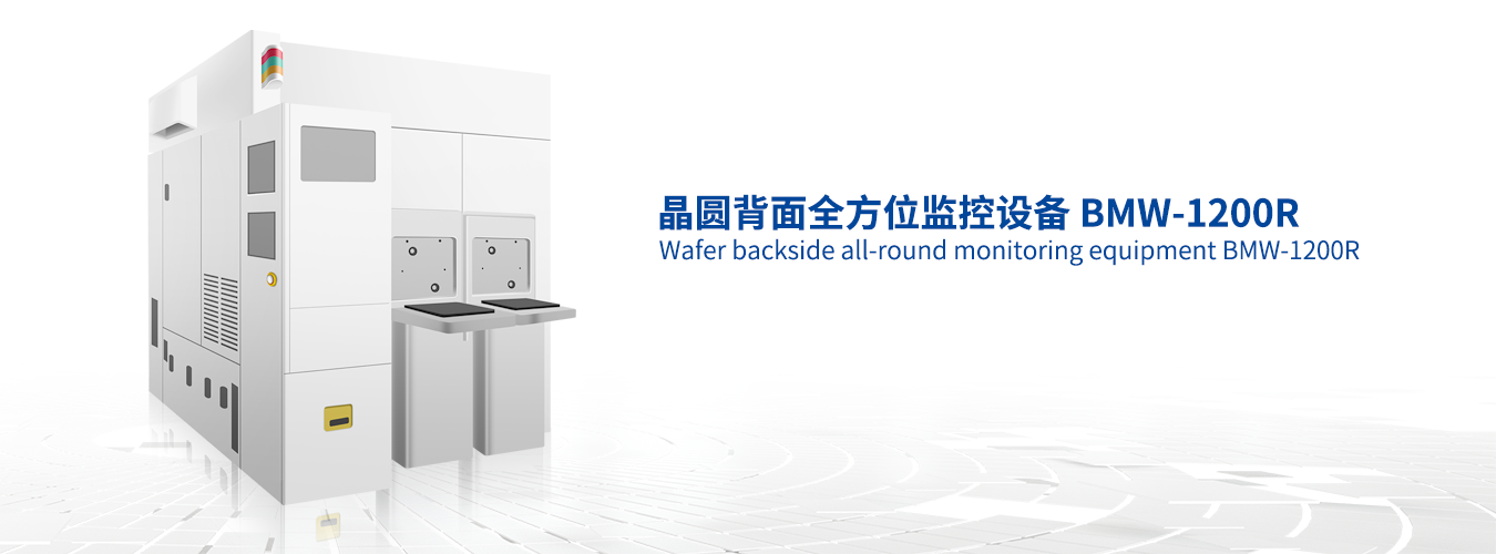
晶圆背面全方位监控设备 BMW-1200R
优点介绍
得到国际&国内客户端认可的背面监控设备
自研缺陷检测算法+深度学习结合,自动缺陷Review(ADR)和自动缺陷分类(ADC)
在线Review Inspection ,输出彩色图像
晶圆片背面全方位检测,最小检测缺陷0.2um
背面缺陷检测, 8大工艺皆可实现全方位监控
A comprehensive edge monitoring device recognized by international and domestic clients
Combining self-developed defect detection algorithm with deep learning, automatic defect review (ADR) and automatic defect classification (ADC)
Online Review Inspection, output color images
Full directional inspection of back of the wafer, with a minimum detection defect of 0.2um
Back defect inspection, all 8 major processes can achieve all-round monitoring
参数配置
搭载自有3台高清相机实现晶圆的背面检测搭载自研光学架构和光学系统实现自动缺陷检测
搭载扫描式激光显微镜实现缺陷2D&3D信息输出
搭载多种倍率物镜,实现倍率自动切换
集成式EFEM, 设备尺寸更小
设备已通过SEMI认证
Equipped with 3 high-definition cameras to achieve backside inspection of wafers
Equipped with self-developed optical architecture and optical system to achieve automatic defect detection
Equipped with scanning laser microscope to achieve defect 2D&3D information output
Equipped with multiple magnification objectives to achieve automatic magnification switching
Integrated EFEM with smaller device size
The device has passed SEMI certification
功能描述
适用产品:半导体用12寸晶圆, W2W bonding晶圆适用工艺段:DRAM Flash工艺 / Flash工艺 / AP工艺
功能说明:
1.EFEM单元支持FOSB/FOUP/OC等人工或OHT自动上料
2.晶圆的边缘缺陷检测和尺寸量测全方位监控
3.缺陷类型包括:Scratch、Crack、Chuck Mark、Chip、Pin Mark 、Circle-Defect、Particle 、Halo 、Cloud and Haze 、EPI specified defects等
4.量测包括:缺陷的2D&3D形貌尺寸
Applicable products: 12 inch semiconductor wafers, W2W bonding wafers
Applicable process segments: DRAM Flash process/Flash process/AP process
Function Description:
1. The EFEM unit supports manual or OHT automatic feeding such as FOSB/FOUP/OC
2. Comprehensive monitoring of edge defect detection and size measurement of wafers
3. Defect types include Scratch, Crack, Chuck Mark, Chip, Pin Mark, Circle Defect, Particle, Halo, Cloud and Haze, EPI specific defects, etc
4. Measurement includes: 2D&3D morphology and size of defects

