


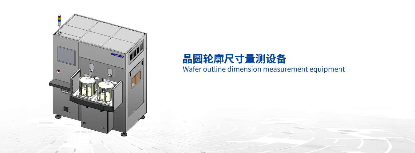
晶圆轮廓尺寸量测设备
优点介绍
第一代硅晶圆轮廓量测已得到国内客户认可,正在研发第二代SIC晶圆倒角轮廓尺寸量测
采用自主研发量测模块以及自主研发算法实现高精度量测&数据分析
对标国外设备商,数据精度更高
设备量测重复精度<1um
The first generation of Si wafer contour measurement has been recognized by domestic customers, and the second generation of SIC wafer character measurement is currently under development
Using independently developed measurement modules and algorithms to achieve high-precision measurement and data analysis
Benchmarking with foreign equipment suppliers for higher data accuracy
Equipment measurement repeatability accuracy<1um
参数配置
搭载自主光路设计+高精度数字测微计实现晶圆自动引导定位采用自主研发高精密对位校准平台
搭载自主光路设计+高清相机实现晶圆轮廓量测
集成式EFEM, 设备尺寸更小
Equipped with independent optical path design and high precision micrometer to achieve automatic wafer guidance and positioning
Adopting self-developed high-precision alignment calibration platform
Equipped with independent optical path design and high-definition camera to achieve wafer contour measurement
Integrated EFEM with smaller device size
功能描述
适用产品:半导体用6/8/12寸硅晶圆/SIC晶圆适用工艺段:倒角/边抛/表面研磨 / 表面抛光 / 清洗 / 终检等
功能说明:
1.EFEM单元支持FOSB/FOUP/OC人工或AGV自动上料
2.高清相机自动引导定位
3.高精度测微计实现直径等尺寸量测
4.高清相机实现晶圆轮廓量测
Applicable products: 6/8/12 inch semiconductor Si wafers, SIC wafer
Applicable process segments: Chamfering/edge polishing/surface grinding/surface polishing/cleaning/final inspection, etc
Function Description:
1. The EFEM unit supports manual or OHT automatic feeding such as FOSB/FOUP/OC
2. HD camera automatically guides positioning
3. High precision micrometer for measuring diameters and other dimensions
4. High definition camera for wafer contour measurement

