


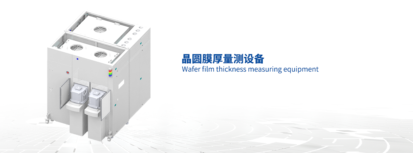
晶圆膜厚量测设备
优点介绍
搭配SE+SR两种测量模式
波长范围广,支持190nm ~ 1100nm
测量范围广,1nm-100μm
测量层数多,1~10层
重复精度高,0.03nm
测量速度快,<1s / point
Paired with SE+SR measurement modes
Wide wavelength range, supporting 190nm~1100nm
Wide measurement range, 1nm-100 μ m
Multiple measurement layers, 1-10 layers
High repeatability accuracy, 0.03nm
Fast measurement speed,<1s/point
参数配置
搭载SE椭偏仪和SR分光干涉测厚仪配合高精度相机引导定位,实时观测
搭配双port或多port EFEM单元对接OHT&AMR实现全自动上下料
Equipped with SE ellipsometer and SR spectroscopic interferometer thickness gauge
Cooperate with high-precision camera guidance for positioning and real-time observation
Paired with dual or multiple port EFEM units to dock with OHT&AMR for fully automatic loading and unloading
功能描述
适用产品:半导体8/12寸有图形晶圆适用工艺段:薄膜沉积、光刻胶、激光开槽、划片切割等
功能说明:
1.EFEM单元支持FOSB/FOUP/OC等人工或OHT上料
2.高清相机引导定位
3.SE/SR模式切换,自动测量膜厚度、光学常数
Applicable products: Semiconductor 8/12 inch patterned wafer
Applicable process segments: Thin film deposition, photoresist, laser slotting, wafer cutting, etc
Function Description:
1. The EFEM unit supports manual or OHT automatic feeding such as FOSB/FOUP/OC
2. High definition camera guided positioning
3. SE/SR mode switching, automatic measurement of film thickness and optical constants

