


MO检查设备
优点介绍
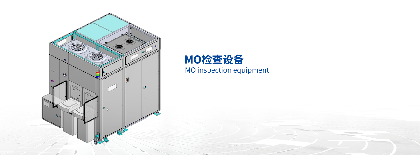
高端半导体制造中必要的缺陷检测装置
采用非破坏、非接触的方式,测量抛光后300 mm硅晶圆近表面层缺陷、异物和雾度
在测量过程中,可监测和记录表面的散射图像
检测缺陷尺寸10nm~30nm
Necessary defect detection devices in high-end semiconductor manufacturing
Non destructive and non-contact methods are used to measure defects, foreign objects, and haze in the near surface layer of polished 300 mm silicon wafers
During the measurement process, scattering images of the surface can be monitored and recorded
Detecting defect sizes ranging from 10nm to 30nm
参数配置
搭载自主光路设计+高性能线扫面阵两用相机采用2种不用波长的激光光源
采用1.25X、2.5X、5X、10X、50X多种物镜自动切换
搭配双port或多port EFEM单元对接OHT&AMR实现全自动上下料
Equipped with independent optical path design and high-performance line scanning array dual-purpose camera
Using two different wavelength laser light sources
Adopting automatic switching of 1.25X, 2.5X, 5X, 10X, and 50X multi axis objective lenses
Paired with dual or multiple port EFEM units to dock with OHT&AMR for fully automatic loading and unloading
功能描述
适用产品:半导体用12寸硅晶圆适用工艺段:表面研磨 / 表面抛光 / 清洗 / 终检等
功能说明:
1.EFEM单元支持FOSB/FOUP/OC人工或AGV自动上料
2.采用激光散射原理,实现晶圆的全面测量
3.检测晶圆表面异物、粗糙、划痕等,检测表面以下(0~5um)内部结晶缺陷
4.具有激光标记功能
Applicable products: 12 inch silicon wafers for semiconductors
Applicable process segments: surface grinding/surface polishing/cleaning/final inspection, etc
Function Description:
1. EFEM unit supports FOSB/FOUP/OC manual or AGV automatic feeding
2. Using laser scattering principle to achieve comprehensive measurement of wafers
3. Detect foreign objects, roughness, scratches, etc. on the surface of the wafer, and detect internal crystal defects below the surface (0-5um)
4. Equipped with laser marking function

